- 您现在的位置:买卖IC网 > Sheet目录3878 > DSPIC30F2010T-20I/SO (Microchip Technology)IC DSPIC MCU/DSP 12K 28SOIC
dsPIC30F
Flash
Programming
S
p
ecification
DS70102K-
page
16
2010
Microchip
T
echnolo
gy
Inc.
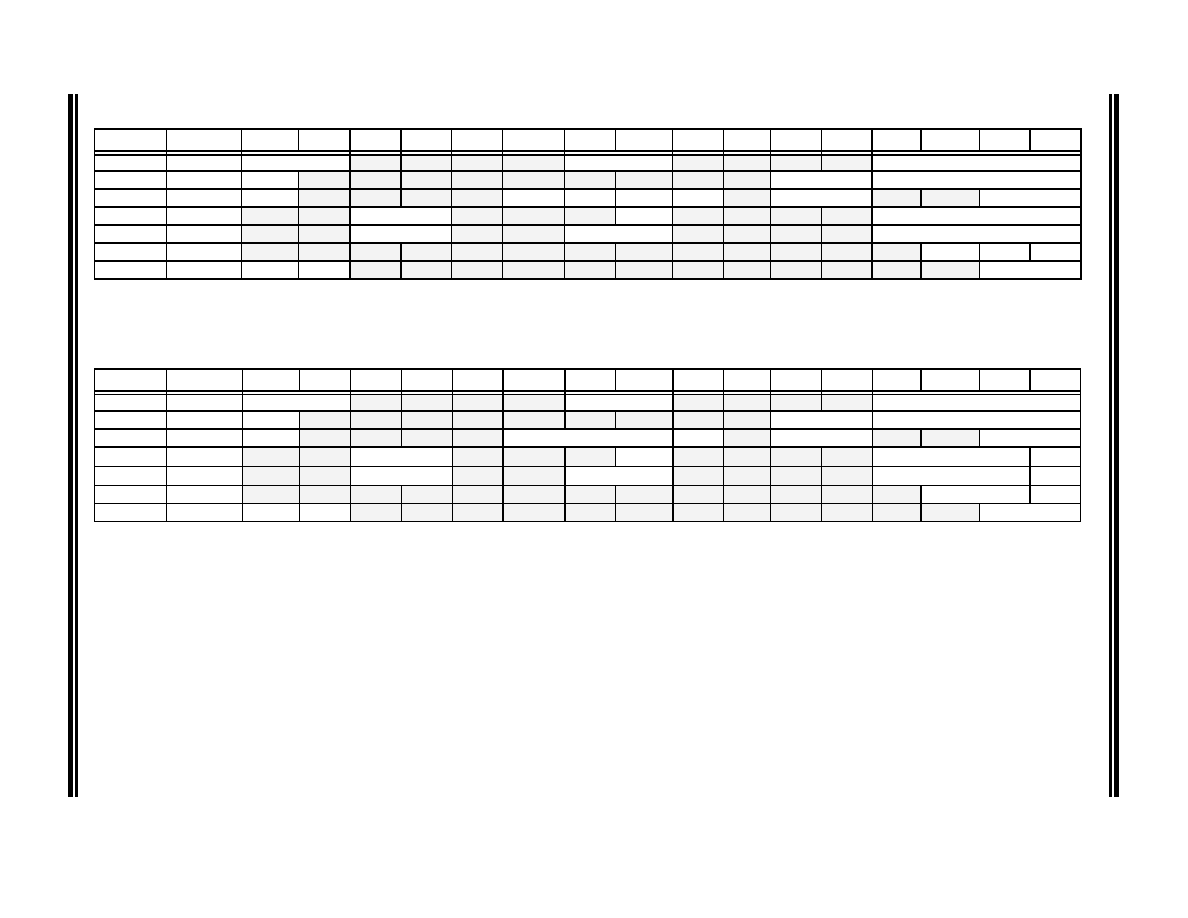
TABLE 5-8:
dsPIC30F CONFIGURATION REGISTERS (FOR dsPIC30F2010, dsPIC30F4011/4012 AND dsPIC30F6010/ 6011/6012/6013/
6014)
Address
Name
Bit 15
Bit 14
Bit 13
Bit 12
Bit 11
Bit 10
Bit 9
Bit 8
Bit 7
Bit 6
Bit 5
Bit 4
Bit 3
Bit 2
Bit 1
Bit 0
0xF80000
FOSC
FCKSM<1:0>
—
FOS<1:0>
—
FPR<3:0>
0xF80002
FWDT
FWDTEN
—
FWPSA<1:0>
FWPSB<3:0>
0xF80004
FBORPOR
MCLREN
—
PWMPIN(1) HPOL(1)
LPOL(1)
BOREN
—
BORV<1:0>
—
FPWRT<1:0>
0xF80006
FBS
—
Reserved(2)
—
Reserved(2)
—
Reserved(2)
0xF80008
FSS
—
Reserved(2)
—
Reserved(2)
—
Reserved(2)
0xF8000A
FGS
—
Reserved(2)
GCP
GWRP
0xF8000C
FICD
BKBUG
COE
—
ICS<1:0>
Note
1:
On the 6011, 6012, 6013 and 6014, these bits are reserved (read as ‘1’ and must be programmed as ‘1’).
2:
Reserved bits read as ‘1’ and must be programmed as ‘1’.
TABLE 5-9:
dsPIC30F CONFIGURATION REGISTERS (FOR dsPIC30F5011/5013)
Address
Name
Bit 15
Bit 14
Bit 13
Bit 12
Bit 11
Bit 10
Bit 9
Bit 8
Bit 7
Bit 6
Bit 5
Bit 4
Bit 3
Bit 2
Bit 1
Bit 0
0xF80000
FOSC
FCKSM<1:0>
—
FOS<1:0>
—
FPR<3:0>
0xF80002
FWDT
FWDTEN
—
FWPSA<1:0>
FWPSB<3:0>
0xF80004
FBORPOR
MCLREN
—
Reserved(1)
BOREN
—
BORV<1:0>
—
FPWRT<1:0>
0xF80006
FBS
—
RBS<1:0>
—
EBS
—
BSS<2:0>
0xF80008
FSS
—
RSS<1:0>
—
ESS<1:0>
—
SSS<2:0>
0xF8000A
FGS
—
GSS<1:0>
GWRP
0xF8000C
FICD
BKBUG
COE
—
ICS<1:0>
Note
1:
Reserved bits read as ‘1’ and must be programmed as ‘1’.
BWRP
SWRP
发布紧急采购,3分钟左右您将得到回复。
相关PDF资料
PIC18F24J10-I/SP
IC PIC MCU FLASH 8KX16 28-DIP
PIC18LF23K22-I/SO
IC PIC MCU 8KB FLASH 28SOIC
PIC16F639-E/P
IC MCU FLASH 2KX14 20DIP
PIC12F635T-I/MF
IC MCU FLASH 1KX14 8DFN
PIC12F635-E/MF
IC MCU FLASH 1KX14 8DFN
DSPIC30F6014T-20I/PF
IC DSPIC MCU/DSP 144K 80TQFP
DSPIC30F6013T-20I/PF
IC DSPIC MCU/DSP 132K 80TQFP
DSPIC30F6012T-30I/PF
IC DSPIC MCU/DSP 144K 64TQFP
相关代理商/技术参数
DSPIC30F2010T-20I/SOG
功能描述:数字信号处理器和控制器 - DSP, DSC DIG SIG CONTR Lead Free Package RoHS:否 制造商:Microchip Technology 核心:dsPIC 数据总线宽度:16 bit 程序存储器大小:16 KB 数据 RAM 大小:2 KB 最大时钟频率:40 MHz 可编程输入/输出端数量:35 定时器数量:3 设备每秒兆指令数:50 MIPs 工作电源电压:3.3 V 最大工作温度:+ 85 C 封装 / 箱体:TQFP-44 安装风格:SMD/SMT
dsPIC30F2010T-30I/MM
功能描述:数字信号处理器和控制器 - DSP, DSC 16B MCU DSP 28LD 20MIPS 12KB FLASH RoHS:否 制造商:Microchip Technology 核心:dsPIC 数据总线宽度:16 bit 程序存储器大小:16 KB 数据 RAM 大小:2 KB 最大时钟频率:40 MHz 可编程输入/输出端数量:35 定时器数量:3 设备每秒兆指令数:50 MIPs 工作电源电压:3.3 V 最大工作温度:+ 85 C 封装 / 箱体:TQFP-44 安装风格:SMD/SMT
DSPIC30F2010T-30I/MMG
功能描述:数字信号处理器和控制器 - DSP, DSC 16 Bit MCU/DSP 28LD 30M 12KB FL RoHS:否 制造商:Microchip Technology 核心:dsPIC 数据总线宽度:16 bit 程序存储器大小:16 KB 数据 RAM 大小:2 KB 最大时钟频率:40 MHz 可编程输入/输出端数量:35 定时器数量:3 设备每秒兆指令数:50 MIPs 工作电源电压:3.3 V 最大工作温度:+ 85 C 封装 / 箱体:TQFP-44 安装风格:SMD/SMT
DSPIC30F2010T-30I/SO
功能描述:数字信号处理器和控制器 - DSP, DSC 20MHz 12KB Flash RoHS:否 制造商:Microchip Technology 核心:dsPIC 数据总线宽度:16 bit 程序存储器大小:16 KB 数据 RAM 大小:2 KB 最大时钟频率:40 MHz 可编程输入/输出端数量:35 定时器数量:3 设备每秒兆指令数:50 MIPs 工作电源电压:3.3 V 最大工作温度:+ 85 C 封装 / 箱体:TQFP-44 安装风格:SMD/SMT
DSPIC30F2010T-30I/SOG
功能描述:数字信号处理器和控制器 - DSP, DSC 16 Bit MCU/DSP 28LD 30M 12KB FL RoHS:否 制造商:Microchip Technology 核心:dsPIC 数据总线宽度:16 bit 程序存储器大小:16 KB 数据 RAM 大小:2 KB 最大时钟频率:40 MHz 可编程输入/输出端数量:35 定时器数量:3 设备每秒兆指令数:50 MIPs 工作电源电压:3.3 V 最大工作温度:+ 85 C 封装 / 箱体:TQFP-44 安装风格:SMD/SMT
DSPIC30F2011
制造商:MICROCHIP 制造商全称:Microchip Technology 功能描述:High-Performance, 16-Bit Digital Signal Controllers
DSPIC30F2011_06
制造商:MICROCHIP 制造商全称:Microchip Technology 功能描述:High-Performance, 16-Bit Digital Signal Controllers
DSPIC30F2011_08
制造商:MICROCHIP 制造商全称:Microchip Technology 功能描述:High-Performance, 16-bit Digital Signal Controllers